Most of the home brewers and electronics hobbyist see fabricating a PCB as a roadblock . I will describe an alternate approach to circuit construction where you need only bare copper clad sheet. This method is some times called Manhattan method.( I don’t know the reason.)
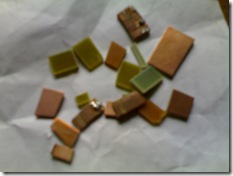
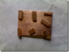
The basic ingredients you need for this type of construction is bare copper clad sheet. Either glass epoxy or paper phenolic boards can be used. As the first step take a small pieces of copper clad sheet and chip it into small pads. There is no minimum size or maximum size . Use a sharp tool like a chisel for cutting the board. Some sample pieces that I made is shown in the figure below. If you have access to a sheet metal cutting tool, it is very easy to make them. I keep a small box of such PCB chips.
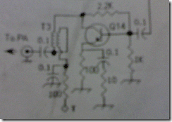
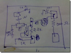
Collect all the components that you need for construction. Study the circuit you are planning to build and make a rough layout of component placement on paper. Pay special attention to the size and shape of the components you are planning to use. If possible, make the circuit layout section by section . This will make debugging easier. The circuit will be fabricated on a a plain copper clad sheet .The copper clad sheet will be the ground of your circuit Keep this in mind when you make the sketch. Here is the circuit and a rough sketch I made for constructing bitx20. ( This is RF preamplifier stage of bitx20).
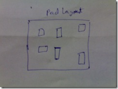
Make a pad layout next from the above layout.
The size of the copper clad sheet needed can be roughly estimated if you have some idea about the components. Cut a sufficiently large piece of copper clad and then clean it properly. Affix the pads using super glue. Any other adhesive used in electronic repair can be used.
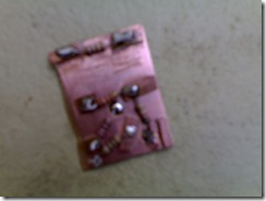
Now start soldering . Make sure that the pads are clean. I use a sharp knife to clean the pads. Start with the resistors. Keep the leads small.. Next , solder the capacitors followed by other low foot print components.
Finally, fix the transistors. You circuit is ready for testing .
There are several advantages to this type of construction. The plain copper clad sheet will act as a ground plane and will improve the performance of RF circuits. Also, If you want to replace a faulty component it is very easy.
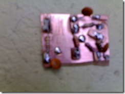
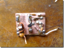
Hello sir,
I am not sure abt this, but the name might have come from the term Manhattanization, which is a term used to describe construction of dense, orderless high rise buildings in a city…
the circuit almost looks like this :p
http://en.wikipedia.org/wiki/Manhattanization
I fear,though it was and is practiced in certain parts, it is too crude a system. Better that our youth learn a pcb making by other means.
Even a marker pen way of PCB drafting would make it a better practice, even though etching might tale little more time.
a small circular annular tool can make pads easily. than using pcb chips stuck to substrate etc as done in manhattan way.
No insult intended, but this is a terrible way of building a circuit. Especially if you want it to last. Just go a and make your own printed circuit boards. Today it is easy and cheap to make professional looking PCBs with a computer (your on one now), PCB software (free ones here http://www.rdrop.com/~cary/mirror/tools_htmlized.html#PCB), laser printer (most people have access to one), and a kit from http://www.pulsarprofx.com for under $200. After you have the required hardware, your PCBs will cost you less than $.30 US per square inch.